List of Contributors
1Pulsed Laser Deposition for Complex Oxide Thin Film and Nanostructure
1.1Introduction
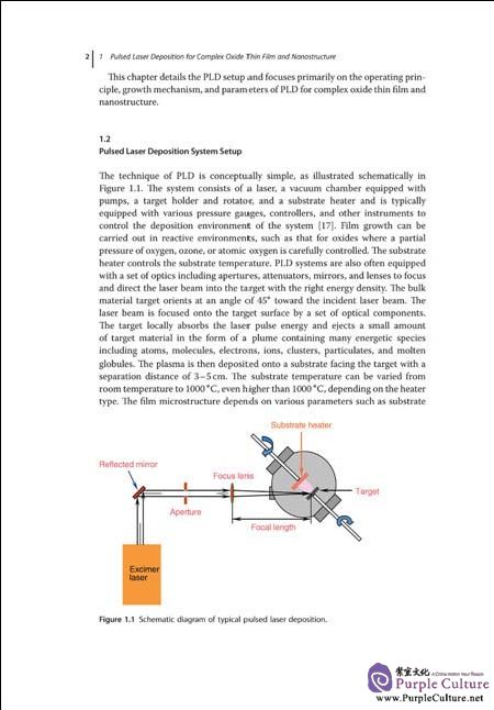
1.2Pulsed Laser Deposition System Setup
1.3Advantages and Disadvantages of Pulsed Laser Deposition
1.4The Thermodynamics and Kinetics of Pulsed Laser Deposition
1.4.1Laser—Material Interactions
1.4.2Dynamics of the Plasma
1.4.3Nucleation and Growth of the Film on the Substrate Surface
1.5Monitoring of Growth Kinetics
1.5.1Introduction and RHEED Studies
1.5.2Growth Kinetics Studies by Surface X —ray Diffraction
1.6Fundamental Parameters in Thin Film Growth
1.6.1Substrate Temperature
1.6.2Background Gas Pressure
1.6.3Laser Fluence and Ablation Area
1.6.4Target—Substrate Distance
1.6.5Post—Annealing
1.6.6Lattice Misfit
1.7Pulsed Laser Deposition for Complex Oxide Thin FilmGrowth
1.7.1Pulsed Laser Deposition for Superconductor Thin Film
1.7.2Pulsed Laser Deposition for Ferroelectric Thin Films
1.7.3Pulsed Laser Deposition for Ferromagnetic Thin Film
1.7.4Pulsed Laser Deposition for Multiferroics Thin Film
1.7.5Interface Strain Engineering the Complex Oxide Thin Film
1.7.5.1Thickness Effect
1.7.5.2Substrate Effect
1.7.5.3Post—Annealing
1.8Pulsed Laser Deposition for Nanostructure Growth
1.8.1Self—Assembled Nanoscale Structures
1.8.2Geometrically Ordered Arrays
1.9Variation of Pulsed Laser Deposition
1.10Conclusion
References
2Electron Beam Evaporation Deposition
2.1Introduction
2.2Electron Beam Evaporation System
2.2.1Heating Principle and Characters of Electron Beams
2.2.1.1Heating Principle of Electron Beams
2.2.1.2Characters of Electron Beams
2.2.2Equipments of Electron Beam Source
2.2.2.1Filament and Electron Emission
2.2.2.2Electron Beam Control
2.2.2.3Power Supply, Crucibles, and Feed Systems
2.2.2.4Source Materials
2.2.3Application of Electron Beam Evaporation
2.2.3.1Cooling of Electron Beam Gun
2.2.3.2Evaporation of Source Materials by Electron Beam
2.2.3.3Vacuum Deposition Process of Electron Beam Evaporation
2.2.3.4Attention and Warning for Electron Beam Evaporation
2.3Characterization of Thin Film
2.3.1Surface Morphology by AFM
2.3.2Thickness Measurement by Spectroscopic Ellipsometry
2.4Summary
Acknowledgments
References
3 Nanostructures and Thin Films Deposited with Sputtering
3.1Introduction
3.2Nanostructures with Sputtering
3.2.1Oxide Nanostructures
3.2.1.1Needle—Shaped MoO3 Nanowires
3.2.1.2Bi2O3 Nanowires
3.2.2Nitride Nanostructures
3.2.2.1Graphitic—C3N4 Nanocone Array
3.2.2.2InAIN Nanorods
3.3Thin Films Deposited with Sputtering
3.3.1Metal Alloy Thin Films
3.3.1.1LaNi5 Alloy Ihin Films
3.3.1.2Ni—Mn—In Alloy Thin Films
3.3.2Composite Metal Oxide Thin Films
3.3.2.1BiFeO3/BaTiO3 Bilayer Thin Films
3.4Summary
Acknowledgments
References
4Nanostructures and Quantum Dots Development with Molecular Beam Epitaxy
4.1Introduction
4.2Technology of MBE
4.2.1The Physics of MBE
4.2.2MBE Growth Mechanisms
4.2.2.1Two—Dimensional (2D) MBE Growth Mechanism
4.2.2.2Three—Dimensional (3D) MBE Growth Mecharusm
4.2.2.3Stranskie—Krastanow 3D Growth Mechanism
4.3Nanoheterostructures Fabricated by Molecular Beam Epitaxy
4.3.1Semiconducting Oxide Heterostructures Grown by Laser MolecularBeam Epitaxy
4.3.2Strain—Induced Magnetic Anisotropy in Highly Epitaxial Heterostructure by LMBE
4.4Quantum Dots Development with Molecular Beam Epitaxy
4.5Summary
Acknowledgments
References
5Carbon Nanomaterials and 2D Layered Materials Development withChemical Vapor Deposition
5.1Introduction
5.2Carbon Nanotube Synthesis by Chemical Vapor Deposition
5.2.1Overview of CVD Process of Carbon Nanotube Growth
5.2.2Control of Carbon Nanotube Structure
5.2.3The Alignment of Carbon Nanotube Array
5.3Graphene Synthesis by Chemical Vapor Deposition
5.3.1Overview of CVD Process of Graphene Synthesis
5.3.2Control of Graphene Quality
5.4Metal Dichalcogenide Synthesis by Chemical Vapor Deposition
5.4.1Overview of CVD Process of Metal Dichalcogenides
5.4.2Growth Control of Metal Dichalcogenides in Chemical Vapor Deposition
5.5Summary
References
6Nanostructures Development with Atomic Layer Deposition
6.1Introduction
6.2Reaction Mechanisms
6.2.1Thermal ALD
6.2.2Catalytic ALD
6.2.3Metal ALD
6.3 Nanostructures Based on ALD
6.3.1Nanolaminates and Nanofilms
6.3.2Nanostructures as Templates
6.3.3Nanostructured Modification
6.4Summary
Acknowledgments
References
7Nanomaterial Development with Liquid—Phase Epitaxy
7.1Introduction
7.2Hydrothermal Method
7.2.1Development of Hydrothermal Method
7.2.2Microwave—Assisted Hydrothermal Method
7.2.2.1Microwave—Assisted Preparation of Nanostructures in Aqueous
7.3Nanostructures Fabricated Using LPE
7.3.1Core—Shell Structures
7.3.2The Epitaxial Preparation Methods of Core—Shell Structures
7.3.2.1General Nanochenucal Approaches to Prepare Epitaxial Core—ShellUCNPs with a Single Shell Layer
7.3.2.2Layer—by—Layer Approach to Prepare Core—Multishell UCNPs withMonolayer Thickness Precision
7.3.2.3Mesoporous Silica Coating
7.3.2.4Coupling of UCNPs with Plasmonics Using Core—Shell Architecture
7.4Summary
Acknowledgments
References
8NanostructuraIThin Film Development with Chemical Solution Deposition
8.1Introduction
8.2Precursor Solution Preparation
8.2.1Chemical Strategies for Precursor Solutions
8.2.2Sol—Gel Method
8.2.3Metal—Organic Deposition
8.2.4Polymer—Assisted Deposition
8.3Coating
8.4Thermal Treatment
8.5Control of the Microstructures in 'lhin Films Prepared by CSD Techniques
8.5.1Thermodynamics for CSD—Delivered Thin Films
8.5.2Epitaxial Thin Film Growth
8.6 Examples of Nanostructural Thin Films Prepared by CSD Techniques
8.6.1Sol—Gel—Delivered Nanostructured Materials
8.6.2MOD of Nanostructured Materials
8.6.3PAD—Delivered Nanostructured Materials
8.7Summary
References
……
9Nanomaterial Development Using In Situ Liquid Cell TransmissionElectron Microscopy
10Direct—Writing Nanolithography
113D Printing of Nanostructures
12Nanostructured Thin Film Solid Oxide Fuel Cells
13Nanostructured Magnetic Thin Films and Coatings
14Phase Change Materials for Memory Application
15Nanomaterials and Devices on Flexible Substrates
Index


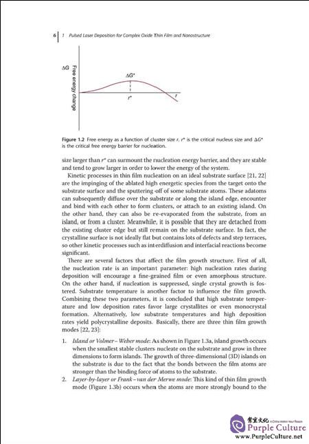


")
")
")
")
")
")
")


")
")


")
